Ok, you tumbled over my On-Wafer Measurements and Calibration – part I blog post and have already some first idea of what we are talking about….
You have your setup ready, your cables and probes mounted on the probe station and want to proceed?

Well, you are ready to go and all you need is to calibrate properly your Network Analyzer. Now you want to get in more depth and need to understand better the concept of Calibration and how to set up your Network Analyzer?
Let’s begin with the definition of Calibration and what is the impact for your Network Analyzer… In order to put it in simple words, Calibration is the mathematical procedure of removing imperfection in the test system and is performed prior to the actual device under test (DUT) measurements!
How to perform On-Wafer Calibration?
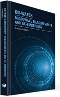
Ok, here is the deal… you need proper calibration standards that will be provided by the probe manufacturer. Usually, it comes in the form of a ceramic substrate with printed gold patterns on it. Those patterns form well defined devices, called here calibration standards, whose electrical performance is known.
To get an idea of how this looks like… here is an example of an ISS (Impedance Standard Substrate) from Cascade Microtech.
![ISS Calibration Substrate [Courtesy of Cascade Microtech]](https://i0.wp.com/www.lourandakis.com/wp-content/uploads/2014/09/ISS-300x222.png?resize=300%2C222)
ISS Calibration Substrate [Courtesy of Cascade Microtech]
Those standards together with the parasitics from the RF probes to be used will be the most significant input parameters in the calibration process.
Well, we got it, we need all that for the calibration procedure… but how is the calibration performed?
Thruth is, there are several calibration routines available that rely on different error models and terms. Short-Open-Load-Thru (SOLT), Thru-Reflect-Line (TRL), and Line-Reflect-Reflect-Match (LRRM) are probably the most used calibration routines out there.
We shall not dive here into all the details of each calibration algorithm, this would be way beyond the scope of these posts. The backbone of all the calibration routines is to measure the aforementioned well know calibration standards and perform a set of calculations for the associated error terms.
Ok, let’s assume you performed the calibration at your best and want to validate the results… Hmm, what can you do to validate a calibration?
Remember, the calibration will move the electrical reference plane at your probe tips, in other words… the calibrated measurements will appear as they are launched directly at your probe tips. In this context, one safe procedure is to measure some of the verification structures on the calibration substrate.
Validation of On-Wafer Calibration
Here is my advice, after you have performed the calibration raise your probes in the air and measure the reflection coefficient S11 and S22 with the Network Analyzer. 
What do you expect to get? Well, since you measure an OPEN you would like to see a perfect reflection… translated to S-parameters you would expect |S11| –> 0 dB.
In practice when your S11, S22 reflection look like that and is within the boundaries of -0.1dB and 0.1dB … you should be fine!
![]()
If you want to get deeper into that… measure the Open Stub T-line at the lower part of the ISS in a 1-port configuration.
Your S11 in this case should look like this when observed in the Smith Chart. You want to see a trace that moves inwards and in clockwise direction on the Smith Chart. No crossovers and obviously… no trace outside of the Smith Chart.
Make sure your validation measurements look like that…. and your calibration is done!
Sign up for the RF Measurements Newsletter and get the latest news!